With the increase in complexity of FPGA device capabilities and the associated designs targeting these FPGA devices, in-system debug can quickly become a bottleneck in the FPGA design cycle. This article describes a methodology that can help reduce the in-system debug cycle and improve the quality of your design.
The debug of any type of semiconductor device that is operating in-system can be a challenging and nerve racking experience. You cross your fingers, power up your board, the FPGA loads with your design and nothing happens—or at least not the behavior that you expected to see. Deep down inside, you knew this would happen, but you hoped that everything would function perfectly the first time.
You were too busy designing to the latest changes in specification to consider how to debug the different features in the design while it is running in-system. You now start the stressful and tedious task of trying to isolate the problem within the device that is running, possibly by stripping out parts of the design and trying to shoehorn in debug logic or an FPGA vendor Embedded Logic Analyzer (ELA).
This can be a slow and laborious task involving long delays waiting for FPGA compilations to finish in order to obtain new design images to debug. Seasoned veterans have been through the pressure of debugging designs many times and want to minimize the time spent in this high-pressure environment. They avoid spending evenings and weekends in the lab trying to determine the cause of the problem.
But how is this accomplished? It’s simple: plan for debug up front. Combine some of the techniques that are commonly used in ASIC design with the advantages provided by hardware programmability and the in-system debug tools that are provided by the FPGA vendor. This delivers the best of both worlds.
In-system debug requirements should be built into the specification for an FPGA design. This should cover how each of the major blocks in the design should be verified in-system. Also included should be information on the typeof data that can be viewed to determine that the block is operating as intended. This could include system-level statistics such as the efficiency of memory interfaces, performance bottleneck analysis on buses and bit error ratio information on high-speed transceiver interfaces. The specification will detail the techniques and tools that will be used as part of the in-system debug process to capture the information. This includes information on how many pins, how much logic, how much memory is reserved for in-system debug, and where FPGA debug tools should be used versus user-created debug logic.
The definition of the debug strategy should also include the channel to be used for accessing debug data. The ELAs that are provided by the major FPGA vendors typically use JTAG as the channel for debug. The design engineer needs to determine how to extract data from their debug logic that they have used in the design. They can use device pins, hook it up to the ELA, or design their own debug channel. One technique is to use a soft processor to control the debug process and access the debug data.
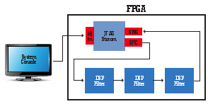 |
| Figure 1: Sample application of an in-system debug via the SystemConsole utility |
The user debug logic provides a good starting point in identifying the area of the design where the problem manifests. It helps to avoid numerous recompiles of the design in trying to isolate the problem. Altera provides a utility, called SystemConsole, for accessing user-created debug logic via an API. It is effectively an interactive console for low-level system debug of designs over various communication channels, including JTAG and TCP/IP. It also provides read and write access to the debug IP in the design via a set of TCL-based commands as shown in Figure 1.
Once the problem area has been identified, the user can then use the FPGA vendor-provided ELAs to further refine the analysis of the problem. This will require incremental compiles of the design, however the number of design recompiles should be substantially fewer than trying to identify the problem without initial debug data.
Following is an In-System Debug Checklist to ensure successful verification of your design.
In-System Debug Checklist
1. Plan for debug
a. Reserve logic and memory resources for Embedded Logic Analyzer (ELA) use.
b. Ensure that you use the JTAG interface to the FPGA.
c. Place a Header on the Board as an interface to an external logic analyzer or scope.
a. Reserve logic and memory resources for Embedded Logic Analyzer (ELA) use.
b. Ensure that you use the JTAG interface to the FPGA.
c. Place a Header on the Board as an interface to an external logic analyzer or scope.
d. Reserve pins for debug.
e. Add debug logic to your design or consider using the FPGA vendor utilities for forcing data to memories and multiplexing data at the pins.
e. Add debug logic to your design or consider using the FPGA vendor utilities for forcing data to memories and multiplexing data at the pins.
f. Consider adding a soft processor to your design for debug.
2. Perform debug
a. Lock down the design implementation using incremental compilation.
b. For free running data, or for a small handful of control signals, incrementally route the signals to pins for analysis on a logic analyzer or scope.
c. In order to capture data based on events, add an ELA to your design. Where possible, use post-fit signal names to avoid a full recompile of the design.
d. If there are multiple devices within the JTAG chain, select the device that you want to target.
3. Recreate the problem in RTL simulation
a. Once you have identified the bug, fix the RTL and validate that the fix works with functional simulation.
In summary, FPGA design debug does not need to be a last minute panic. You can reduce your FPGA design debug cycle time by using a combination of planning for debug and utilizing FPGA vendor supplied debug tools.
Further details on FPGA debug techniques are available in the book “FPGA Design: Best Practices for Team Based Design”, by Phil Simpson. Springer Publishing, 2010.
About the Author
Phil Simpson is Altera’s senior manager for software technical marketing, product planning, and EDA relationships. In this role, he is responsible for Altera’s Quartus II software and third-party EDA interfaces product planning and the creation of the Altera design flow software roadmap. Prior to joining Altera in 1997, Phil held several engineering roles at various EDA and semiconductor companies, including EDA Solutions, Data I/O, and Graseby Microsystems. He holds a B.S. (with honors) in Electrical & Electronic Engineering from City University, London and an M.S.C. (with distinction) in system design from the University of Central England, Birmingham, England. Phil is a published book author on team-based FPGA design. In addition he has written and had published numerous technical articles on topics related to his experience.s on topics related to his experience. ■


1 comment:
Hai sob ,,, linknya sudah sy pasang di blog saya ya sob,maaf klo lama balasnya , tks ya sob
Post a Comment