Mulailah

Tanpa permulaan, anda tidak akan sampai ke mana-mana.

Semangat

Semangat yang kuat mampu mengatasi apapun cobaan yang datang.

Konsisten

Lumbung emas dalam diri kamu adalah pikiran kamu. Kamu dapat menggalinya sedalam-dalamnya dan sepuas-puas yang kamu inginkan.

Pantang Menyerah

Gagal selepas usaha adalah hikmah, anda akan mendapat sesuatu yang lebih besar daripada apa yang anda sangkakan.

Be The One

Be the one is better than be the best.

Monday, February 20, 2012

A Plan For Debug

With the increase in complexity of FPGA device capabilities and the associated designs targeting these FPGA devices, in-system debug can quickly become a bottleneck in the FPGA design cycle. This article describes a methodology that can help reduce the in-system debug cycle and improve the quality of your design.

The debug of any type of semiconductor device that is operating in-system can be a challenging and nerve racking experience. You cross your fingers, power up your board, the FPGA loads with your design and nothing happens—or at least not the behavior that you expected to see. Deep down inside, you knew this would happen, but you hoped that everything would function perfectly the first time. 

You were too busy designing to the latest changes in specification to consider how to debug the different features in the design while it is running in-system. You now start the stressful and tedious task of trying to isolate the problem within the device that is running, possibly by stripping out parts of the design and trying to shoehorn in debug logic or an FPGA vendor Embedded Logic Analyzer (ELA).
 
This can be a slow and laborious task involving long delays waiting for FPGA compilations to finish in order to obtain new design images to debug. Seasoned veterans have been through the pressure of debugging designs many times and want to minimize the time spent in this high-pressure environment. They avoid spending evenings and weekends in the lab trying to determine the cause of the problem.
 
But how is this accomplished? It’s simple: plan for debug up front. Combine some of the techniques that are commonly used in ASIC design with the advantages provided by hardware programmability and the in-system debug tools that are provided by the FPGA vendor. This delivers the best of both worlds.
 
In-system debug requirements should be built into the specification for an FPGA design. This should cover how each of the major blocks in the design should be verified in-system. Also included should be information on the typeof data that can be viewed to determine that the block is operating as intended. This could include system-level statistics such as the efficiency of memory interfaces, performance bottleneck analysis on buses and bit error ratio information on high-speed transceiver interfaces. The specification will detail the techniques and tools that will be used as part of the in-system debug process to capture the information. This includes information on how many pins, how much logic, how much memory is reserved for in-system debug, and where FPGA debug tools should be used versus user-created debug logic.

The definition of the debug strategy should also include the channel to be used for accessing debug data. The ELAs that are provided by the major FPGA vendors typically use JTAG as the channel for debug. The design engineer needs to determine how to extract data from their debug logic that they have used in the design. They can use device pins, hook it up to the ELA, or design their own debug channel. One technique is to use a soft processor to control the debug process and access the debug data.
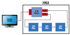
Figure 1: Sample application of an in-system debug via
the SystemConsole utility

The user debug logic provides a good starting point in identifying the area of the design where the problem manifests. It helps to avoid numerous recompiles of the design in trying to isolate the problem. Altera provides a utility, called SystemConsole, for accessing user-created debug logic via an API. It is effectively an interactive console for low-level system debug of designs over various communication channels, including JTAG and TCP/IP. It also provides read and write access to the debug IP in the design via a set of TCL-based commands as shown in Figure 1.

Once the problem area has been identified, the user can then use the FPGA vendor-provided ELAs to further refine the analysis of the problem. This will require incremental compiles of the design, however the number of design recompiles should be substantially fewer than trying to identify the problem without initial debug data. 

Following is an In-System Debug Checklist to ensure successful verification of your design.
 
In-System Debug Checklist

1. Plan for debug
a. Reserve logic and memory resources for Embedded Logic Analyzer (ELA) use.
b. Ensure that you use the JTAG interface to the FPGA.
c. Place a Header on the Board as an interface to an external logic analyzer or scope.
d. Reserve pins for debug.
e. Add debug logic to your design or consider using the FPGA vendor utilities for forcing data to memories and multiplexing data at the pins.
f. Consider adding a soft processor to your design for debug.

2. Perform debug
a. Lock down the design implementation using incremental compilation.
b. For free running data, or for a small handful of control signals, incrementally route the signals to pins for analysis on a logic analyzer or scope.
c. In order to capture data based on events, add an ELA to your design. Where possible, use post-fit signal names to avoid a full recompile of the design.
d. If there are multiple devices within the JTAG chain, select the device that you want to target.

3. Recreate the problem in RTL simulation
a. Once you have identified the bug, fix the RTL and validate that the fix works with functional simulation.

In summary, FPGA design debug does not need to be a last minute panic. You can reduce your FPGA design debug cycle time by using a combination of planning for debug and utilizing FPGA vendor supplied debug tools.
 
Further details on FPGA debug techniques are available in the book “FPGA Design: Best Practices for Team Based Design”, by Phil Simpson. Springer Publishing, 2010.
 
About the Author
 
Phil Simpson is Altera’s senior manager for software technical marketing, product planning, and EDA relationships. In this role, he is responsible for Altera’s Quartus II software and third-party EDA interfaces product planning and the creation of the Altera design flow software roadmap. Prior to joining Altera in 1997, Phil held several engineering roles at various EDA and semiconductor companies, including EDA Solutions, Data I/O, and Graseby Microsystems. He holds a B.S. (with honors) in Electrical & Electronic Engineering from City University, London and an M.S.C. (with distinction) in system design from the University of Central England, Birmingham, England. Phil is a published book author on team-based FPGA design. In addition he has written and had published numerous technical articles on topics related to his experience.s on topics related to his experience. ■

Wednesday, February 15, 2012

The “ground” ; Myth in Printed Circuit Boards

The term “ground” is probably the most misused and misunderstood term in EMC engineering, and in fact, in all of circuit design. Ground is considered to be a zero potential region with zero resistance and zero impedance at all frequencies. This is just not the case in practical high-speed designs. The one thing that should be remembered whenever the term “ground” is used, is that “Ground is a place where potatoes and carrots thrive!” By keeping this firmly in mind, many of the causes of EMC problems would be eliminated.

Figure 1: Initial two board configuration
Figure 2: Return current paths for initial configuration
The term “ground” is a fine concept at DC voltages, but it just does not exist at the frequencies running on today’s typical boards. All metal has some amount of resistance, and even if that resistance was near zero ohms, the current flowing through a conductor in a loop creates inductance. Current through that inductance results in a voltage drop. This means that the metal ground plane/wire/bar/etc. has a voltage drop across it, which is in direct contradiction with the intention and definition of ground The important point is that for EMI/EMC we need to consider the current, not the voltage, in our signal paths. Since current must always flow in a loop back to its source, the return current path must be considered as well as the intended signal path along a PCB trace. Any interruptions to the return current path can have serious negative effects to
the EMI/EMC performance of a PCB. A very slight deviation in return current path can result in enough inductance to dramatically increase emissions.
The return current path is also very important when considering mother/daughter board configurations. Figure 1 shows a simple four-layer board example of a mother/daughter board configuration and a signal path from the mother board to the daughter card through a connector. If we consider how the return current will flow from this configuration, we should expect that the return current will spread out to include displacement current through the dielectric between GND and PWR, as well as local decoupling capacitors (depending on their distance and the plane separation).
Figure 2 shows the return current for this configuration. The added return current path length results in additional inductance in the total path, resulting in a ‘noise’ voltage between the two GND planes (across the connector). This noise voltage will drive the wide, thin, monopole-like antenna, resulting in increased emissions.
However, if we had simply considered the return current path and routed the signal trace so that it was referenced to the same plane (PWR or GND), the return currents are able to stay close to the signal trace (Figure 3), and emissions are greatly reduced.
When we consider the return current path, more ‘ground’ is not always the ‘right’ answer! For example, on a recent design, there was a 144 pin connector with many high speed signals traveling from one board to the other. It was determined that 30 pins could be used for ‘power’ and ‘ground’ combined. At least five pins must be ‘power’ so there would not be an excessive DC voltage drop across the connector. How many of the remaining 25 pins should be ‘ground’?
Figure 3: Improved return current design
In this particular design, it turned out that about 2/3 of the total signal pins were referenced to the ‘power’ plane, and only 1/3 referenced against the ‘ground’ plane. This meant that of the total 30 possible power/ground pins, 2/3 should be ‘power’ and only 1/3 should be ‘ground’! More ‘ground’ pins was NOT the best design for this case. Of course, once we consider both the ‘power’ and the ‘ground’ pins to be return current paths, it is obvious we should distribute them throughout the signal pins to keep the return current deviation as small as possible (compared to putting all the ‘ground’ pins at the ends of the connector, etc.).
When we consider the most important concerns for good EMI/ EMC design, the schematic is not as important as the physical layout of the signal path and the return current. Since today’s high speed PCBs have many layers and are very complex, it is difficult for an engineer to examine each critical signal path for a good return current path. Automated EMC rule checking tools can examine each net in turn, regardless of the PCB complexity. The key to selecting an automated rule checking tool is to make sure it can interface well with your existing design process, it is easy to use, and it can display rule violations in a graphical and easy to understand manner.
The most important EMC design rules for high speed PCBs concern the return current path. Since the return current will always find a path that minimizes the inductance of that path, the return current will always flow on the nearest plane,whether it is called ‘ground’ or ‘power’ or ‘carrots’. When traces across a split in the return plane (for example if a trace is routed next to a power layer with multiple power islands), the return current’s path is interrupted. Changing layers within the PCB so that the return current must also change planes will also interrupt the return current path. Remember, the return current must always get back to its source. It will get back to its source. The only question is whether it will be a path that is beneficial to you, or if it will cause problems. So, “Do you feel lucky today?” It is always best to design ‘on purpose’ rather than ‘by luck’.

About the Author
Dr. Bruce Archambeault


Dr. Bruce Archambeault is an IBM Distinguished Engineer at IBM in Research Triangle Park, NC and co-founder of Applied EM Technology. He received his BSEE degree from the University of New Hampshire in 1977 and his MSEE degree from Northeastern University in 1981. He received his PhD from the University of New Hampshire in 1997. His doctoral research was in the area of computational electromagnetics applied to real-world EMC problems.

Monday, February 13, 2012

The Future Of 8-bit microcontrollers in-home elderly care

What is the right technology solution for a huge global need? Statistically speaking, our world faces a looming crisis that, while it doesn’t hit the headlines often, will eventually affect every single person on our planet, and in crucial ways. The crisis? Our aging population – and an avalanche of need that could likely fall upon the shoulders of us all.

Not enough money, nowhere near enough elderly care facilities, and a changing world that leaves many elderly people with nowhere to turn. These are the symptoms of a population of adults over age 65 that is growing at three times the rate of the population of family members that are available to care for them. Observing the growth rate of the world’s fast-aging population suggests that those who experience middle age in the year 2050 will be three times more likely than they are now to be responsible for the care of many of the projected two billion-plus elderly. These are stark numbers, and yet these numbers are increasing at an alarming rate; they suggest that many elderly will require some level of assistance but have no one around to help.
 
As we get older, several natural tendencies may occur: Folks are not as active as they once were; they may often be sedentary, sitting and reading or watching television more than they did before. These are not bad things, certainly, but we’ve already learned that prolonged periods without physical movement can result in insufficient exercise, which can subsequently lead to other types of health problems. Often, people become more forgetful as they age, and even forgetting simple things such as taking the medicine, feeding the cat, or even scheduling a grocery delivery can ultimately lead to a lack of independence.
 
In addition, it’s not unrealistic to predict that a large percentage of people will reach a point in which they will prefer to “age in place.” People who have worked all of their lives to own their home simply want to stay in it as long as possible. However, they will need a little help to remain independent – help that can also lighten the demand for costly services. That’s where newemerging technologies can play a meaningful role. Many people, as they age, are facing challenges that are completely new to them, and they will simply need a little technological help ensure that their healthcare needs are met.
 
So just what is the solution that can not only assist overburdened caregivers, but even allow the aged to remain longer in their own homes and stay independent at managing their own healthcare needs?

Imagine a smart 8-bit microcontroller that can enable people to live independently, for much longer, and without requiring additional support from the healthcare systems that are currently in place. Indeed, an MCUcontrolled sensor installed in an aging parent’s home could detect patterns which, when they vary from the norm, could be set to alert a remote healthcare service to respond and/or intervene when needed. While privacy could be a concern in such a situation, safeguards could be built into such a monitoring system for assisted living in order to allow people to stay in their own homes longer. Isn’t that a far better alternative than being uprooted and moved to a care facility where you may not feel as comfortable?
 
Let’s look at a set of microcontroller-based sensors which could cover a gamut of situational needs for folks desiring to continue living in their own homes. For example, the safe monitoring process mentioned above could allow a caregiver to “check in” and observe simple lifestyle patterns that would help to make determinations and suggestions for ensuring a person’s quality of life.
 
Having a smart, scalable “independent living network” in place can assist with many everyday tasks by providing reminders or warnings which can inform a person that, for example, the tea on the stove is boiling over. Getting a little reminder about that doctor’s appointment scheduled for this afternoon can lead to better personal healthcare management. Many of these “technical helpers” merely require a microcontroller to process information based on the function(s) for which they are designed. By design, these technical helpers can be interconnected to provide a platform solution that can assist elderly living, with the end result being a person’s self-determined path to stay independent far longer.
 
Tomorrow’s need is already on us today, yet 8-bit microcontrollers will play a far larger role than many now imagine. The actions we take today will be the ones we ourselves will live with tomorrow, through creative solutions that leverage smart MCUs. As a result, we will protect not only our aging loved ones who can then enjoy a better quality of life, but we will also creatively leverage those wonderful microcontrollers so that we, like our parents, can live more independently in the future.
 
What is the right technology solution for a huge global need? Statistically speaking, our world faces a looming crisis that – while it doesn’t hit the headlines often – will eventually affect every single person on our planet, and affect us in crucial ways. The crisis? Our aging population – and an avalanche of need that could likely fall upon the shoulders of us all. 

About the Author 
Steve Darrough is Vice President of Marketing at IXYSZilog. Steve joined Zilog in 2008. Steve possesses more than twenty years of technical engineering and marketing management experience, leading branding and marketing programs. Prior to coming onboard with Zilog, Steve held marketing management and technical engineering roles at Intel Corporations for over 14 years where he had several teams driving new technologies directly relating to the current products initiatives. His teams drove worldwide programs in evangelizing new technologies and accelerate adoption. Steve has a Marketing Degree from the University of Oklahoma.